
Polysilicon:
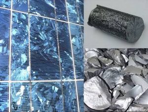
The Ministry of New and Renewable Energy (MNRE) announced that it is formulating a dedicated subsidy scheme to establish 30 GW of domestic polysilicon manufacturing capacity by 2030.
- Polycrystalline silicon (commonly referred to as polysilicon or poly-Si) is a high-purity, hyper-refined crystalline form of elemental silicon composed of multiple microscopic crystallites separated by grain boundaries.
- It serves as the fundamental upstream raw material and chemical feedstock for producing solar photovoltaic (PV) ingots/wafers and semiconductor integrated circuits.
- Mined quartz or silica sand (SiO2) is reduced with carbon sources (coke, charcoal) in a submerged electric arc furnace at temperatures around 1,900 degree C to produce metallurgical silicon of 98–99% purity.
- The pulverized MG-Si is reacted with hydrogen chloride gas at elevated temperatures to form volatile Trichlorosilane or monosilane.
- The liquid trichlorosilane undergoes multi-stage fractional distillation to strip out microscopic traces of metal impurities, boron, and phosphorus.
Chemical Vapor Deposition (Siemens Process / FBR): In the dominant Siemens process, purified TCS mixed with hydrogen is fed into high-temperature reactor bell jars, chemically decomposing to deposit hyper-pure polysilicon onto heated silicon filament rods. Alternatively, continuous Fluidized Bed Reactor (FBR) technology produces granular beads at lower energy consumption.
Key Characteristics of Polysilicon:
- Ultra-High Chemical Purity: Categorized into:
- Solar-Grade (SoG-Si): Purity ranging from 6N to 9N (99.9999% to 99.9999999%).
- Electronic/Semiconductor-Grade (EG-Si): Extreme purity from 9N to 11N (99.999999999%), where foreign impurity atoms are limited to less than 1 part per billion (ppb).
- Capital &Energy-Intensive Production: Demands massive continuous electricity supply and capital expenditure to maintain high-temperature furnaces and complex closed-loop recycling loops.
- Semiconductor & Optical Bandgap Properties: Possesses an intrinsic electronic bandgap that makes it an optimal semiconductor base for converting incident solar photon energy into electric currents via the photovoltaic effect.
- Polycrystalline Morphology: Characterized by internal crystallographic grain boundaries with random orientations, which are melted and re-crystallized via the Czochralski (Cz) growth process to pull single-crystal (monocrystalline) ingots.