
India Semiconductor Mission:
Ministry of Electronics & Information Technology has inaugurated the first ever Semicon India 2022 Conference under India Semiconductor Mission in Bengaluru.
- Semicon India – 2022 has been organized to take forward the vision of the Prime Minister to make India a leader in the electronics manufacturing, semiconductor design, manufacturing & innovation.
- Theme of the Conference: Catalyzing India’s Semiconductor Ecosystem.
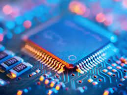
- Semiconductors are Any of a class of crystalline solids intermediate in electrical conductivity between a conductor and an insulator.
- Semiconductors are employed in the manufacture of various kinds of electronic devices, including diodes, transistors, and integrated circuits. Such devices have found wide application because of their compactness, reliability, power efficiency, and low cost.
- As discrete components, they have found use in power devices, optical sensors, and light emitters, including solid-state lasers.
India Semiconductor Mission:
- The ISM was launched in 2021 with a total financial outlay of Rs76,000 crore under the aegis of the Ministry of Electronics and IT (MeitY).
- It is part of the comprehensive program for the development of sustainable semiconductor and display ecosystem in the country.
- The programme aims to provide financial support to companies investing in semiconductors, display manufacturing and design ecosystem.
- Envisioned to be led by global experts in the Semiconductor and Display industry, ISM will serve as the nodal agency for efficient, coherent and smooth implementation of the schemes.
- Components:
- Scheme for setting up of Semiconductor Fabs in India:
- It provides fiscal support to eligible applicants for setting up of Semiconductor Fabs which is aimed at attracting large investments for setting up semiconductor wafer fabrication facilities in the country.
- Scheme for setting up of Display Fabs in India:
- It provides fiscal support to eligible applicants for setting up of Display Fabs which is aimed at attracting large investments for setting up TFT LCD / AMOLED based display fabrication facilities in the country.
- Scheme for setting up of Compound Semiconductors / Silicon Photonics / Sensors Fab and Semiconductor Assembly, Testing, Marking and Packaging (ATMP) / OSAT facilities in India:
- The Scheme provides a fiscal support of 30% of the Capital Expenditure to the eligible applicants for setting up of Compound Semiconductors / Silicon Photonics (SiPh) / Sensors (including MEMS) Fab and Semiconductor ATMP / OSAT(Outsourced Semiconductor Assembly and Test) facilities in India.
- Design Linked Incentive (DLI) Scheme:
- It offers financial incentives, design infrastructure support across various stages of development and deployment of semiconductor design for Integrated Circuits (ICs), Chipsets, System on Chips (SoCs), Systems & IP Cores and semiconductor linked design.
- Scheme for setting up of Semiconductor Fabs in India:
- Vision: To build a vibrant semiconductor and display design and innovation ecosystem to enable India’s emergence as a global hub for electronics manufacturing and design.